Blab AI
Copper Wall Forces AI Data Centers Toward Silicon Photonics
AI workloads now run on racks that house tens of thousands of processors, demanding data exchanges at terabit rates. In these massive stacks, the copper wiring that has linked computers for decades is hitting a hard limit – the so‑called "copper wall." That bottleneck is pushing the industry toward silicon photonics and co‑packaged optics.
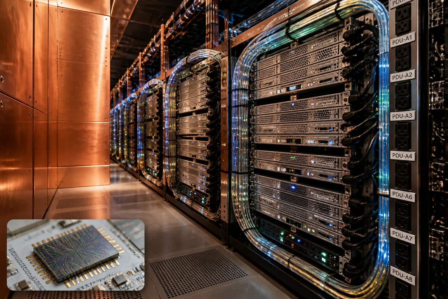
The copper wall stems from copper cables’ inability to preserve clean electrical signals over long distances at the high data rates required for modern AI training. Beyond roughly a meter, signals degrade, forcing more power to maintain integrity. In a single server the effect is minor, but in a warehouse‑sized cluster the cumulative loss caps performance and drives up heat and energy costs.
Silicon photonics replaces copper with light carried through fiber or on‑chip waveguides. Light travels farther, carries more data, and consumes less power over distance, making it ideal for board‑to‑rack links in AI clusters. The most advanced incarnation is co‑packaged optics (CPO), where optical components are fabricated directly beside the switch chip or accelerator. By shrinking the electrical path from inches to millimeters, CPO cuts translation loss and packs higher bandwidth into the same space.
The shift is already attracting sizable investment. Nvidia announced a $6.5 billion commitment to photonics to tackle the copper wall, while silicon‑photonics startup Lumilens noted that copper hits a wall at about 1.6 terabits and roughly a meter as clusters scale toward 400,000 GPUs. In August 2025, AIchip Technologies and Ayar Labs unveiled a CPO solution that extends reach, lowers latency, and increases radix for AI clusters.
Market analysts project rapid growth for optical interconnects in AI data centers. The optical interconnect market for AI is expected to multiply several times over the decade, and the broader optical transceiver market is forecast to jump about 60 % in a single year to roughly $26 billion in 2026. Other forecasts show the inter‑chip optical interconnect market expanding from $18.01 billion in 2025 to $32.73 billion by 2030, and the silicon photonics market scaling from $3–4 billion in 2025–2026 to $10–29 billion by 2030–2034.
Manufacturing capacity is a concern. Global shipments of optical transceivers are projected to more than triple to 92 million units by 2026, up from 26.5 million in 2023, but the industry faces challenges in scaling production to meet demand. The copper wall is not disappearing; it is being relegated to the shortest hops inside a package, while optics will dominate longer‑distance links.
The transition to silicon photonics and CPO is already reshaping data‑center design. Co‑packaged optics solutions promise higher bandwidth, lower power consumption, and reduced latency—critical for training large language models and other AI workloads. As AI clusters grow, the copper wall will become an increasingly pressing issue, and the industry is responding with targeted investments and new product launches.
In short, AI data centers are confronting a copper‑based interconnect ceiling that limits performance and energy efficiency. Silicon photonics and co‑packaged optics offer a path forward, backed by significant corporate investment and strong market growth forecasts. The industry is actively developing and deploying optical solutions while manufacturing capacity expands to support the expected surge in optical transceiver demand.
The copper wall stems from copper cables’ inability to preserve clean electrical signals over long distances at the high data rates required for modern AI training. Beyond roughly a meter, signals degrade, forcing more power to maintain integrity. In a single server the effect is minor, but in a warehouse‑sized cluster the cumulative loss caps performance and drives up heat and energy costs.
Silicon photonics replaces copper with light carried through fiber or on‑chip waveguides. Light travels farther, carries more data, and consumes less power over distance, making it ideal for board‑to‑rack links in AI clusters. The most advanced incarnation is co‑packaged optics (CPO), where optical components are fabricated directly beside the switch chip or accelerator. By shrinking the electrical path from inches to millimeters, CPO cuts translation loss and packs higher bandwidth into the same space.
The shift is already attracting sizable investment. Nvidia announced a $6.5 billion commitment to photonics to tackle the copper wall, while silicon‑photonics startup Lumilens noted that copper hits a wall at about 1.6 terabits and roughly a meter as clusters scale toward 400,000 GPUs. In August 2025, AIchip Technologies and Ayar Labs unveiled a CPO solution that extends reach, lowers latency, and increases radix for AI clusters.
Market analysts project rapid growth for optical interconnects in AI data centers. The optical interconnect market for AI is expected to multiply several times over the decade, and the broader optical transceiver market is forecast to jump about 60 % in a single year to roughly $26 billion in 2026. Other forecasts show the inter‑chip optical interconnect market expanding from $18.01 billion in 2025 to $32.73 billion by 2030, and the silicon photonics market scaling from $3–4 billion in 2025–2026 to $10–29 billion by 2030–2034.
Manufacturing capacity is a concern. Global shipments of optical transceivers are projected to more than triple to 92 million units by 2026, up from 26.5 million in 2023, but the industry faces challenges in scaling production to meet demand. The copper wall is not disappearing; it is being relegated to the shortest hops inside a package, while optics will dominate longer‑distance links.
The transition to silicon photonics and CPO is already reshaping data‑center design. Co‑packaged optics solutions promise higher bandwidth, lower power consumption, and reduced latency—critical for training large language models and other AI workloads. As AI clusters grow, the copper wall will become an increasingly pressing issue, and the industry is responding with targeted investments and new product launches.
In short, AI data centers are confronting a copper‑based interconnect ceiling that limits performance and energy efficiency. Silicon photonics and co‑packaged optics offer a path forward, backed by significant corporate investment and strong market growth forecasts. The industry is actively developing and deploying optical solutions while manufacturing capacity expands to support the expected surge in optical transceiver demand.