Blab AI
South Korean President to Announce $649 Billion Mega-Projects Focused on Honam Semiconductor Cluster
On Monday, President Lee Jae‑Myung will unveil a trio of public‑private initiatives that together promise a staggering 1,000 trillion won—about $649 billion—in investment. The projects target South Korea’s semiconductor industry, artificial‑intelligence data centers, and physical‑AI technologies, with a sharp focus on the southwestern Honam region.
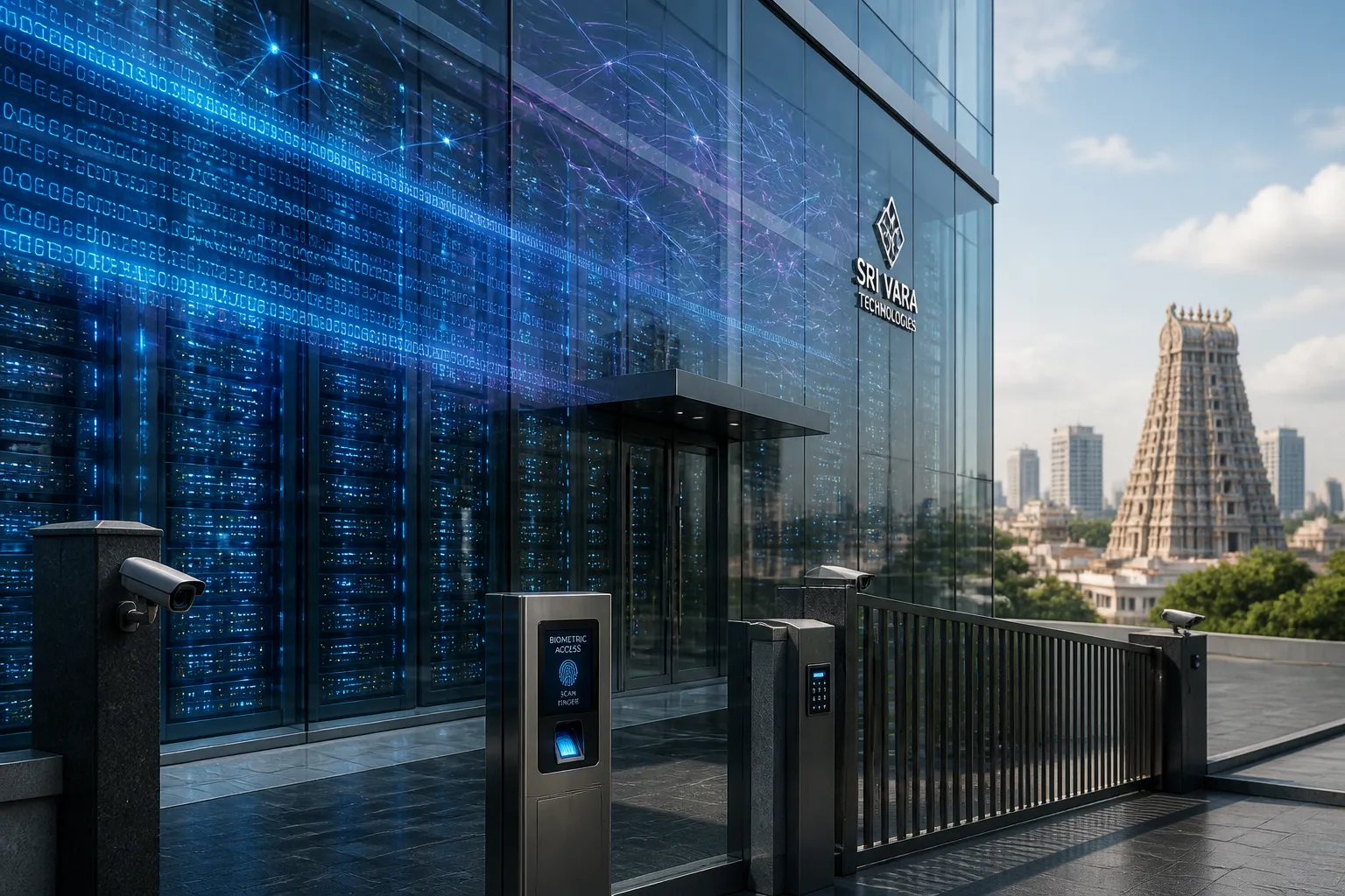
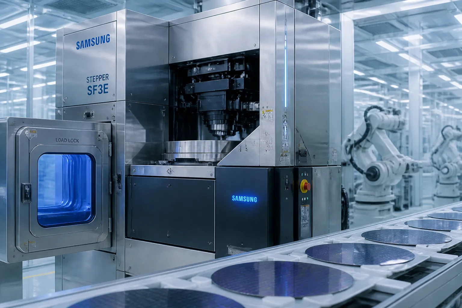
At the heart of the plan is a semiconductor cluster that will be spearheaded by Samsung Electronics and SK Hynix, the country’s two largest memory‑chip makers. The cluster is slated for Gwangju and the surrounding South Jeolla Province, and the government intends to weave semiconductor production with AI data centers and physical‑AI facilities spread across Honam, Chungcheong, and Yeongnam. The goal is to forge an integrated ecosystem that eases Seoul’s dominance in advanced‑technology manufacturing.
President Lee has already laid the groundwork with industry leaders. He met SK Group chairman Chey Tae‑won on 19 June and Samsung Electronics chairman Lee Jae‑yong on 25 June to hash out cooperation on the semiconductor front. According to the presidential office, the talks were designed to align corporate investment plans with the state’s broader strategy.
The People Power Party (PPP), South Korea’s main opposition, has voiced sharp criticism. The party argued that investment decisions should hinge on practical factors—electricity, water, skilled labor, and supplier networks—rather than regional development rhetoric. “Semiconductors are an ecosystem, not an electoral district,” the PPP said, calling for a feasibility assessment of Honam before any funds are committed.
Lee countered the accusations by stressing that the cluster represents a “historic achievement.” He insisted that corporate executives chose to participate because they saw clear business benefits. He also pointed out that Gwangju and South Jeolla Province earned the highest rating in the semiconductor category during a competition to select specialized national high‑tech industry zones under the previous administration.
The presidential office confirmed that the project had already received official backing during the PPP government. Specific sites, investment timelines, and the split of costs between the state and private partners will be revealed during Monday’s briefing.
These projects are part of a larger regional‑development blueprint aimed at diversifying South Korea’s advanced‑technology base. By relocating a major semiconductor hub outside Seoul, the government hopes to spark growth in Honam, Chungcheong, and Yeongnam, and to seed new industrial centers.
The initiative dovetails with the government’s push to expand AI infrastructure. Separate plans have already been announced for AI data centers in Chungcheong and for physical‑AI projects in Yeongnam. Linking these facilities with the semiconductor cluster is intended to create a closed‑loop ecosystem that supports chip design, manufacturing, AI training, and deployment.
While the details are still forthcoming, the announcement signals a firm commitment to large‑scale public‑private investment in South Korea’s high‑technology sector. The projects could reshape the country’s industrial geography, strengthen the domestic semiconductor supply chain, and broaden the AI ecosystem.
As the briefing approaches, analysts will scrutinize how the 1,000 trillion won investment will be allocated, the construction and operation timelines, and the financing split between the state and its corporate partners. The outcome will also reveal how the government balances regional development ambitions with the practical requirements of semiconductor manufacturing.
In short, Monday’s briefing will confirm the scope and execution plan for a $649 billion investment that could bring a new semiconductor cluster to Honam, link it with AI infrastructure across three regions, and potentially shift South Korea’s advanced‑technology landscape away from a Seoul‑centric model.