Blab AI
SK Hynix Accelerates HBM4E Delivery, Offering 48-GB 12-Layer Stacks Ahead of Samsung
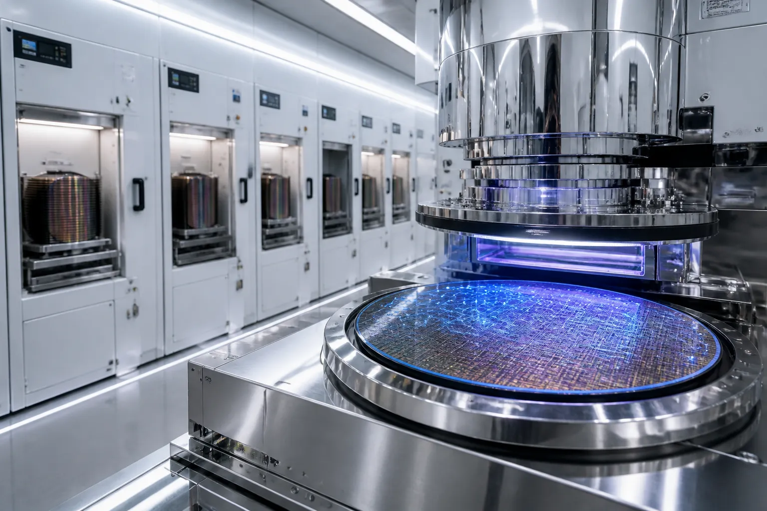
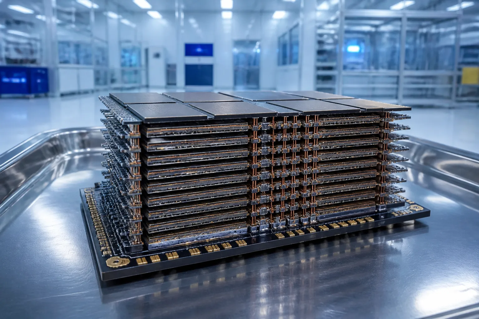
SK Hynix announced on 20 June 2026 that it has begun shipping samples of its 12‑layer high‑bandwidth memory (HBM) product, HBM4E, to major hardware customers. Each stack contains 48 GB of memory, operates at up to 16 Gbps per pin, and delivers roughly 4 TB/s of bandwidth when a single stack is used.
The new HBM4E stacks are built on the JEDEC‑approved HBM4 standard, which was defined in April 2025. SK Hynix’s 12‑layer configuration represents a 30 % increase in capacity over the 4‑layer HBM4 chips that were common in the previous generation. The 2‑kilobit interface width of the HBM4 standard allows the 16‑Gbps per‑pin speed to translate into the high aggregate bandwidth reported.
To address the thermal and power challenges that come with stacking twelve memory dies, SK Hynix has applied its proprietary Advanced Mass Reflow Molded Underfill (MR‑MUF) packaging process. The technique injects a liquid protective material between the stacked chips, which the company says reduces thermal resistance by 17 % compared with standard HBM4 packaging. The same process is reported to improve overall power efficiency by about 20 %, a benefit that is important for data‑center operators that must balance large AI training clusters against limited power budgets.
The timing of the announcement is notable. SK Hynix had originally planned to release HBM4E samples later in the year, but the company moved the schedule forward to mid‑June. The shift appears to be a response to Samsung Electronics, which shipped its own 12‑layer HBM4E samples on 29 May 2026. Samsung’s stacks also provide 48 GB per stack, 16 Gbps per pin, and up to 3.6 TB/s of bandwidth. Both companies are among the “Big Three” memory manufacturers and serve major AI accelerator customers, including NVIDIA.
After delivery, the HBM4E samples will enter a qualification phase. Developers of AI accelerators that target the 2027 product cycle are expected to test the SK Hynix stacks for signal integrity, thermal reliability, and manufacturing yield at scale. The results of these tests will influence the allocation of multi‑billion‑dollar supply contracts for the next wave of AI hardware.
The broader memory market is experiencing intense competition. HBM has become a critical bottleneck for large‑language‑model training and inference, and the demand for higher density, higher bandwidth memory has driven the rapid development of successive HBM generations. SK Hynix’s early delivery of HBM4E samples is a strategic move to secure its position as a primary supplier for high‑performance AI systems.
In summary, SK Hynix’s 12‑layer HBM4E samples provide 48 GB of memory per stack, 16 Gbps per pin, and up to 4 TB/s of bandwidth. The MR‑MUF packaging technique is claimed to lower thermal resistance and improve power efficiency. The samples were shipped earlier than originally planned, likely in response to Samsung’s earlier shipment. The next steps involve rigorous qualification by AI accelerator developers, after which supply contracts for the 2027 cycle will be decided. The outcome will shape the memory supply landscape for the next generation of AI hardware.