Blab AI
Architect Labs Raises $24 Million to Democratize Custom Chip Design
On June 18, 2026, Palo Alto’s Architect Labs announced a $24 million seed round that could change the way custom silicon is engineered. The investment, led by Kindred Ventures and supported by TQ Ventures, Race Capital, Together Fund, and a roster of prominent AI and semiconductor figures, will bankroll the company’s AI‑driven design engine and its first collaborations on production silicon.
The round brought together a mix of venture capital and industry veterans, including Kindred’s managing partner Steve Jang, who joined the board in the wake of the deal. Jang said the company’s mission is “to deliver ultra‑low latency, energy‑efficient, and affordable intelligence at scale by enabling AI labs, robotics makers, and cloud operators to iterate on novel chip hardware at the same pace as model development.” The money will expand compute infrastructure, deepen research, and help the startup partner with early adopters.
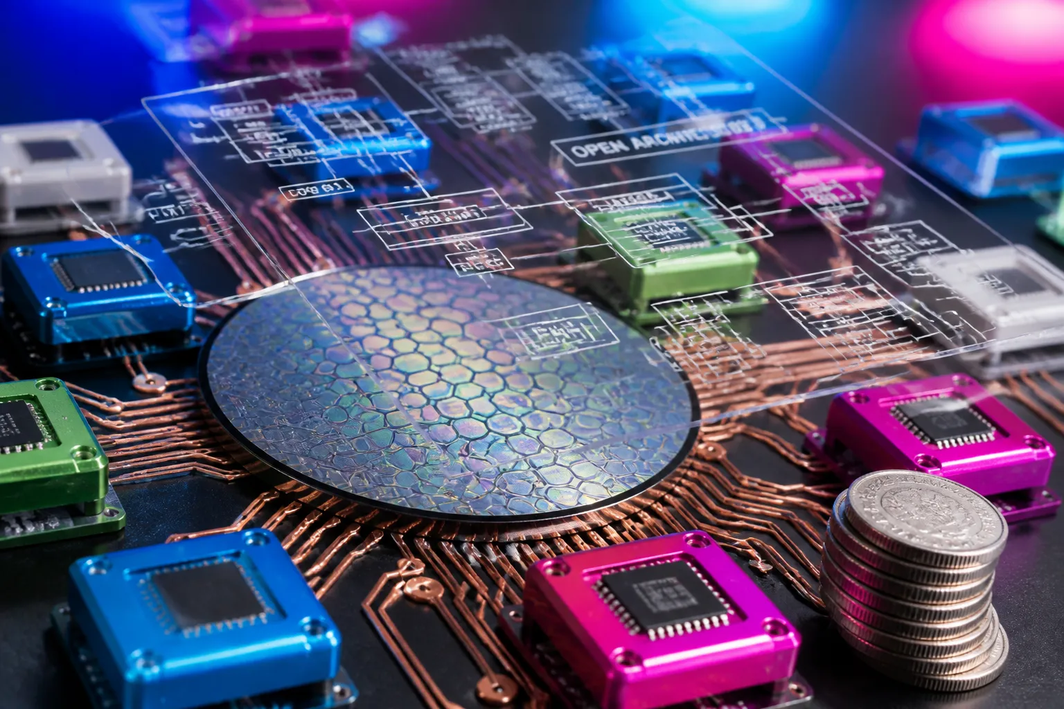
Architect Labs is building an artificial‑intelligence system that can accelerate the design of custom chips and full‑stack silicon solutions for organizations that need hardware beyond off‑the‑shelf options. According to the founders, the rapid growth of AI has shifted computing from a simple GPU‑CPU‑memory configuration to large, integrated environments built around specialized silicon. General‑purpose hardware can no longer keep pace with AI’s complex demands for specialized compute, advanced networking, and high‑speed connections.
Designing a chip remains a gated effort. The founders note that the process typically takes years, costs hundreds of millions, and requires a small pool of experts concentrated in a few companies. Two decades ago, the fabless model let companies design chips without owning a fab; TSMC made world‑class manufacturing available to anyone with a chip design. Architect Labs plans to do the same for design itself, making world‑class chip design available to anyone with a workload.
The startup calls this the “designless semiconductor industry.” The founders say the model would let organizations avoid becoming chip companies, making decade‑long bets on an architecture, or carrying the risk of a failed tape‑out. They also say it would dramatically accelerate the chip development timeline.
Co‑founder Ebrahim Hussain, who left high school early to study at college at 15 and worked on custom chips at Apple and Tesla, said the company’s goal is to unlock AI‑first semiconductor design by rethinking the entire design process from first principles. Hussain co‑founded Architect with Aaditya Subedi, an AI researcher at Harvard. The pair met at Stanford, where their research focused on building AI systems for chip design and verification, and they dropped out of school to start Architect.
The team now includes frontier AI researchers, former professors, chip designers, and systems engineers. The new capital will allow the company to scale its compute infrastructure, deepen its AI research, and co‑design production silicon with early industry partners.
Architect Labs plans to extend its partnership and the capabilities of its AI system across the full computing stack, from silicon to co‑designing compilers, runtimes, system software, and eventually co‑optimizing AI models themselves. The company says that when chip design moves closer to the pace of software, models, architectures, and silicon can be truly co‑optimized together.
The funding round included participation from key figures in modern computing and AI, including Srinivas Narayanan, Lukasz Kaiser, Aravind Srinivas, Kunle Olukotun, Trevor Blackwell, Dr. Alex Wissner‑Gross, Shaad Khan, and executives from NVIDIA, Google, and OpenAI.
Architect Labs’ announcement comes as the semiconductor industry faces increasing pressure to meet AI’s specialized hardware needs. The company’s approach, if successful, could reduce the need for large in‑house chip design teams and lower the risk associated with tape‑out failures.
At present, the startup has not disclosed a product launch date. The company’s next steps, according to reports, include scaling its AI‑driven design platform, securing additional industry partnerships, and expanding its team of researchers and engineers.
In summary, Architect Labs has raised $24 million to build an AI system that could democratize custom silicon design. The company’s leadership, funding sources, and stated goals suggest a focus on accelerating chip development, reducing design risk, and enabling a broader range of organizations to create purpose‑built hardware for AI, robotics, defense, and consumer devices.
The round brought together a mix of venture capital and industry veterans, including Kindred’s managing partner Steve Jang, who joined the board in the wake of the deal. Jang said the company’s mission is “to deliver ultra‑low latency, energy‑efficient, and affordable intelligence at scale by enabling AI labs, robotics makers, and cloud operators to iterate on novel chip hardware at the same pace as model development.” The money will expand compute infrastructure, deepen research, and help the startup partner with early adopters.
Architect Labs is building an artificial‑intelligence system that can accelerate the design of custom chips and full‑stack silicon solutions for organizations that need hardware beyond off‑the‑shelf options. According to the founders, the rapid growth of AI has shifted computing from a simple GPU‑CPU‑memory configuration to large, integrated environments built around specialized silicon. General‑purpose hardware can no longer keep pace with AI’s complex demands for specialized compute, advanced networking, and high‑speed connections.
Designing a chip remains a gated effort. The founders note that the process typically takes years, costs hundreds of millions, and requires a small pool of experts concentrated in a few companies. Two decades ago, the fabless model let companies design chips without owning a fab; TSMC made world‑class manufacturing available to anyone with a chip design. Architect Labs plans to do the same for design itself, making world‑class chip design available to anyone with a workload.
The startup calls this the “designless semiconductor industry.” The founders say the model would let organizations avoid becoming chip companies, making decade‑long bets on an architecture, or carrying the risk of a failed tape‑out. They also say it would dramatically accelerate the chip development timeline.
Co‑founder Ebrahim Hussain, who left high school early to study at college at 15 and worked on custom chips at Apple and Tesla, said the company’s goal is to unlock AI‑first semiconductor design by rethinking the entire design process from first principles. Hussain co‑founded Architect with Aaditya Subedi, an AI researcher at Harvard. The pair met at Stanford, where their research focused on building AI systems for chip design and verification, and they dropped out of school to start Architect.
The team now includes frontier AI researchers, former professors, chip designers, and systems engineers. The new capital will allow the company to scale its compute infrastructure, deepen its AI research, and co‑design production silicon with early industry partners.
Architect Labs plans to extend its partnership and the capabilities of its AI system across the full computing stack, from silicon to co‑designing compilers, runtimes, system software, and eventually co‑optimizing AI models themselves. The company says that when chip design moves closer to the pace of software, models, architectures, and silicon can be truly co‑optimized together.
The funding round included participation from key figures in modern computing and AI, including Srinivas Narayanan, Lukasz Kaiser, Aravind Srinivas, Kunle Olukotun, Trevor Blackwell, Dr. Alex Wissner‑Gross, Shaad Khan, and executives from NVIDIA, Google, and OpenAI.
Architect Labs’ announcement comes as the semiconductor industry faces increasing pressure to meet AI’s specialized hardware needs. The company’s approach, if successful, could reduce the need for large in‑house chip design teams and lower the risk associated with tape‑out failures.
At present, the startup has not disclosed a product launch date. The company’s next steps, according to reports, include scaling its AI‑driven design platform, securing additional industry partnerships, and expanding its team of researchers and engineers.
In summary, Architect Labs has raised $24 million to build an AI system that could democratize custom silicon design. The company’s leadership, funding sources, and stated goals suggest a focus on accelerating chip development, reducing design risk, and enabling a broader range of organizations to create purpose‑built hardware for AI, robotics, defense, and consumer devices.